A civic-education cartridge that runs on a 1985 console. Not an emulator skin and not a retro-styled web page — a 128 KiB ROM, a discrete-logic board, and a printable shell, so a public-records game can be handed to somebody as an object.
The software is OpenArcade, ported from the Perfect World module of the same name. Its original idea — the cabinet is permanent, games are cartridges — turned out to map onto the hardware almost exactly: one 16 KiB program bank is one cartridge slot, and the cabinet lives in the bank the console keeps mapped at all times.
On the cartridge 2 of 4 slots used
Camino Real
A civic survival run north along El Camino Real de Tierra Adentro, a donkey pulling a tarp-covered Cybertruck. Fifteen real stops from El Paso del Norte to Santa Fe, three roles, seven resources, trail and town events, and a public-records deck that trades information against water, food, cash and time.
System Check
The diagnostic cartridge, and the board bring-up tool. Reports mapper, PRG size, CHR-RAM and mirroring; scans all seven swappable banks through the mapper; write/read tests CHR-RAM and work RAM; live controller readout; twelve-colour bar pattern. Run this first on any board you build.
Empty, and wired
Reserved for future cartridges. The unused banks already carry their signatures, so the bank scan proves the whole 128 KiB is reachable before there is anything in it. Adding a game is a new source file and one row in the catalog.
Project area — the board PWP-UNROM-128
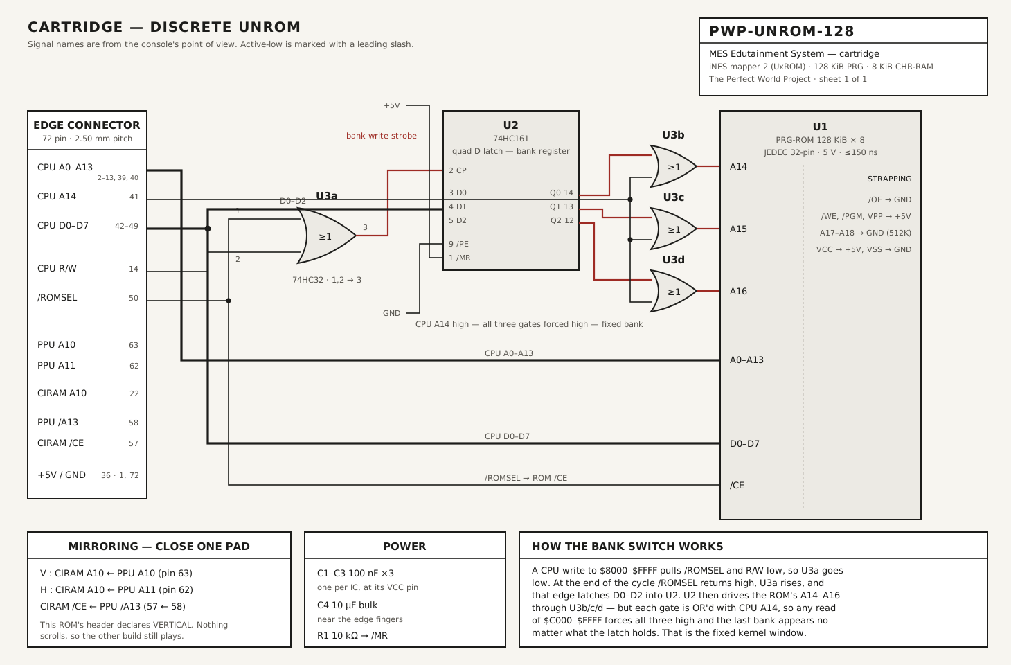
Discrete UNROM, iNES mapper 2. 128 KiB of program ROM in eight 16 KiB banks, with the console supplying 8 KiB of character RAM. Two 74-series chips do the whole job — no mapper ASIC, no CPLD, nothing that needs programming beyond the ROM itself.
Why two chips is the whole mapper
The 74HC161 is a counter used as a four-bit latch: it holds the bank
number. The 74HC32's four OR gates do double duty — one makes the write
strobe from /ROMSEL and R/W, and the other three
OR the latch outputs with CPU A14. That last trick is the
entire fixed-bank mechanism: whenever the processor reads
$C000–$FFFF, A14 is high, all three address lines are forced
high, and the last bank appears no matter what the latch holds.
Bill of materials
| Ref | Part | Package | Note |
|---|---|---|---|
| U1 | PRG-ROM 128 KiB × 8, 5 V, ≤150 ns | JEDEC 32-pin | SST39SF040 or AT28C010 |
| U2 | 74HC161 — 4-bit counter as a quad D latch | DIP-16 / SOIC-16 | the bank register |
| U3 | 74HC32 — quad 2-input OR | DIP-14 / SOIC-14 | strobe + multiplexer |
| C1–C3 | 100 nF ceramic X7R | 0805 | one per IC, at its VCC pin |
| C4 | 10 µF electrolytic or tantalum | — | bulk, near the fingers |
| R1 | 10 kΩ | 0805 | pull-up on /MR |
| PCB | FR-4, gold-flash or ENIG edge fingers | 2.50 mm pitch | 1.2 mm thick, not 1.6 |
| Shell | 3D printed, two halves + 2 × M2×8 | PETG or ABS | parametric source included |
Fabrication quotable now, not buildable yet
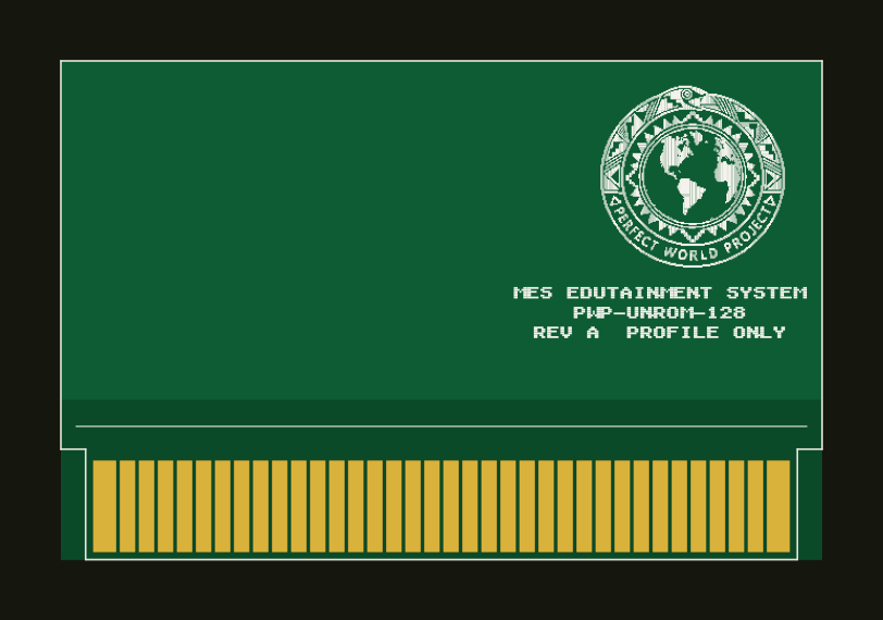
The board is generated by script from measured dimensions rather than drawn by hand, so every number is traceable to a source and a correction regenerates every layer at once. What follows is plotted back from the Gerbers that would be sent — not from the data they came from — so a fault in the output shows up as a wrong picture instead of shipping quietly.
Multi-source by design
Component shortages are the expected failure, not the unlikely one, so the board is not tied to a part number. It targets the signals a 1 Mbit ROM needs and brings the four pins that differ between families out to solder jumpers, so six different ROMs strap onto the same bare board. The logic footprints are overlapping DIP and SOIC, which means one board can be hand-soldered with an iron or machine-assembled for a run — without a respin between them.
What the fabricator has to be told
| Item | Value | Why it matters |
|---|---|---|
| Thickness | 1.20 mm | Every prototype house defaults to 1.6 mm. A 1.6 mm board will not seat, and forcing it splays the console's connector permanently. |
| Gold fingers | Hard gold, 72 fingers, 2.50 mm pitch | ENIG alone is soft plating that wears through after a few dozen insertions. |
| Edge bevel | 30–45° lead-in, both faces | Without it the board chews the connector on insertion. Usually skipped unless asked. |
| Soldermask | None over the tongue | Mask left on a contact finger cannot be fixed after fabrication. |
| Board size | 100.00 × 65.50 mm, 2 layers | From the measured cartridge drawing, not from a guess. |
The one thing still gated
The ROM's pin mapping is the standard JEDEC 32-pin arrangement, but it has not been confirmed against a manufacturer datasheet. Committing remembered pin numbers to fabricated copper is not acceptable, so the generator refuses to emit the full package until that check is recorded. Everything else — outline, card edge, netlist, logic footprints — is independent of it.
Getting the ROM onto a chip three routes
.nes file is 16 bytes of header followed by the ROM. Burn it
as-is and every byte lands 16 addresses late. Burn the
.bin — it must be exactly 131,072 bytes.
Off-the-shelf cartridge
Buy a blank UNROM-512 flash cart and its programmer. That mapper is a superset of ours, so the ROM runs after one repacking step that moves the kernel into the bank the hardware keeps fixed. Fastest path to a physical unit.
Donor cartridge
Because this is stock UNROM/128 KiB, an NES-UNROM donor becomes an MES cartridge by replacing a single chip — no mapper work at all. Contra, Castlevania, Mega Man, Metal Gear and Duck Tales are all suitable. Buy beaters, not boxed copies.
Build the board
Fabricate PWP-UNROM-128 and populate it. Two weeks of lead time and the only route that scales to a run. Do A or B first — prove the ROM on real hardware before anyone places a PCB order.
Acceptance test
Every finished cartridge runs slot 2, System Check before
it gets a label. Bank scan must read OK for banks 0–6 and
KE for the kernel bank; any -- means that bank is
unreachable and the fault is in the latch, the multiplexer, or a ROM
address line. Then CHR-RAM and work RAM must pass, every button must
register, and the colour bars must be clean.
Status honest
- ROM builds — 128 KiB, mapper 2, NES 2.0 header, all bank signatures verified
- Cabinet, insert and eject round trip through the mapper
- System Check passes every self-test in emulation
- Camino Real playable start to finish — full run to Santa Fe, both endings
- Schematic, bill of materials and bring-up procedure written
- Printable shell — both halves manifold, exported, dimensioned
- Board geometry traceable to the measured cartridge drawing, self-checked
- Netlist complete — 39 nets, no pin on two nets, every required pin connected
- Profile package generated and plotted back from its own Gerbers
- ROM pin mapping not yet datasheet-confirmed — generator refuses the full package
- Footprints, placement and routing not done
- No PCB fabricated
- No chip burned
- No shell printed
- Never run on real hardware — the first physical unit is the first hardware test
- Lockout policy undecided: an unmodified front-loader will blink without a CIC
Everything above the line is verified in emulation. Nothing below it has been attempted. The build documentation is written as the script to follow the first time, not as a report of something that already happened.